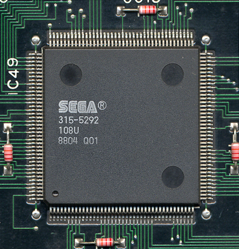
== 仕様 ==
SYSTEM24に実装されていた315-5292

4.) Tilemap generator (315-5292)
The tilemap generator handles two 64x64 playfields, and it looks like
there are two 'window' planes that are probably used for static graphics
like a status bar or menu.

The tilemap generator is mapped to addresses $200000-2FFFFF:

$200000-20FFFF : Name table data (64K)
$280000-2FFFFF : Pattern data (512K space, only 128K available)

The Model 2 hardware uses the same chip with 512K of pattern data RAM. As
the System 24 board only implements 128K, this means that some of the high
order address bits are ignored. Due to mirroring they will appear to do
nothing.

The name table memory is divided into four 8K tables, which are composed
of 64x64 entries, two bytes per entry. I believe the tables are arranged
like so:

$200000-201FFF : Playfield A
$202000-203FFF : Playfield A (Window?)
$204000-205FFF : Playfield B
$206000-207FFF : Playfield B (Window?)
$208000-209FFF : Playfield row/column scroll data (4K word sized values)
$20A000-20BFFF : First 16 words seem to be playfield scroll and control.
$20C000-20DFFF : Unknown (window control?)
$20E000-20FFFF : Unused

The data at offsets $8000-$9FFF seems to be for row or column scrolling.
The data at offsets $C000-$DFFF seems to be a name table sized bitmap
which might be used for enabling the alternate window layer in tile sized
units.

The name table entries have the following format:

MSB          LSB
--nnnnnnnnnnnnnn : Pattern name (Bits 13,12 have no effect, only 128K of RAM)
-pppppppp------- : Palette
?--------------- : Unknown

The patterns are 8x8 pixels, 4 bits per pixel. They are arranged as 4 bytes
per line, 8 lines per pattern, for a total of 32 bytes per pattern. There
is enough memory for 4096 patterns.

If anyone designs a Model 2 emulator with debugging facilities, it might
lead to more insight on how this chip works. (and vice-versa)
Sega 315-5292 tilemap chip (System 24, Model 1)

656 pixels per scanline:
 69 pixels from /HSYNC high to /BLANK high (left border)
496 pixels from /BLANK high to /BLANK low (active display)
 43 pixels from /BLANK low to /HSYNC low (right border)
 48 pixels from /HSYNC low to /HSYNC high (horizontal sync. pulse)

424 scanlines per frame:
 25 scanlines from /VSYNC high to /BLANK high (top border)
384 scanlines from /BLANK high to /BLANK low (active display)
 11 scanlines from /BLANK low to /VSYNC low (bottom border)
  4 scanlines from /VSYNC low to /VSYNC high (vertical sync. pulse)

Using 16 MHz pixel clock, 57.52 frames per second

Setting $270001.b = $01 selects an invalid 512-scanline screen mode (same horizontal timings) where the display is enabled during the vertical sync. pulse and blanked at the wrong time.
Maybe it's an unimplemented feature or used for chip testing, but it's definitely not useful. However it prevents frame buffer autoerase from working properly, so you can draw as many sprites as you want and keep the old ones.
| 端子番号 |
端子名 |
端子機能 |
その他 |
| 1 |
GND |
0V |
|
| 10 |
GND |
0V |
|
| 20 |
VCC |
+5V電源 |
|
| 30 |
GND |
0V |
|
| 41 |
GND |
0V |
|
| 50 |
GND |
0V |
|
| 60 |
VCC |
+5V電源 |
|
| 68 |
CLK1 |
16MHzクロック入力 |
|
| 69 |
CLK2 |
32MHzクロック入力 |
|
| 70 |
GND |
0V |
|
| 80 |
VCC |
+5V電源 |
|
| 81 |
GND |
0V |
|
| 90 |
GND |
0V |
|
| 110 |
GND |
0V |
|
| 121 |
GND |
0V |
|
| 130 |
GND |
0V |
|
| 138 |
VCC |
+5V電源 |
|
| 138 |
RESET# |
リセットパルス入力 |
|
| 140 |
VCC |
+5V電源 |
|
| 141 |
GND |
0V |
|
| 143 |
GND |
0V |
|
| 150 |
GND |
0V |
|
| 155 |
VCC |
+5V電源 |
|
| 160 |
VCC |
+5V電源 |
|
== 外部リンク ==
最終更新:2019年11月12日 00:28
